Contactless solder cleaning methods is rapidly replacing manual cleaning in more and more applications. This white paper will summarize the evolution process.
That’s why Contactless Solder Cleaning is rapidly replacing manual cleaning in increasingly more rework applications.
The PCB rework process has long consisted of three steps:
- Removal of the inoperative component.
- Cleaning of residual solder from the ball grid assembly (BGA) pads which held the inoperative component in place.
- Replacement with a new component to create a viable PCB.
The first and third steps—removal and replacement—have long been automated, and are completed on rework machines with operator assistance. Cleaning, the middle step—and arguably, the most sensitive and vital step when it comes to reclaiming a damaged board—is often done completely manually by a skilled and experienced technician. The cleaning is performed with hand tools, usually a wicking braid and a soldering iron, using standard or specialized tips. The effectiveness of the operation is highly dependent on the skills of the individual operator. With the emphasis often placed on work throughput, board damage is quite common.
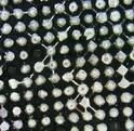
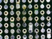
 One common scenario in manual cleaning is the destruction of a pad due to sticking, when the heat of the soldering iron momentarily dissipates through the board, causing the delicate pad to stick to the wick and be chipped or lifted off the board entirely when the operator pulls the tool back. Overwhelming, destruction to a pad results in a wasted, scrap board.
Today, increasing, in the drive to help smartphone, tablets and other emerging products deliver greater functionality, manufacturers are creating thicker PCBs with multiple inner layers of copper. These, unfortunately, also cause the heat to dissipate more and more quickly when using hand held cleaning tools, ensuring that sticking challenges will become even more problematic going forward.
 Other risks to the circuit board assembly when performing a manual BGA cleaning are numerous:
- Molten solder can flow into electrical connections and vias, causing shorts in the PCB.
- Solder can be removed inconsistently among the dozens or hundreds of pads, resulting in poor adhesion of the new component.
- Portions of the solder can be inadvertently removed by the wick, causing solder to flow into electrical connections when the board is put back into the rework machine, leading to bridges and shorts.
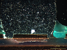
Another potential issue, which is not discernible by the naked eye, or even x-ray inspection, is creation of pad craters in the fiberglass under the pad. These issues arise mainly due to stresses caused by the operator:
- Molten solder can flow into electrical connections and vias, causing shorts in the PCB.
- Solder can be removed inconsistently among the dozens or hundreds of pads, resulting in poor adhesion of the new component.
- Portions of the solder can be inadvertently removed by the wick, causing solder to flow into electrical connections when the board is put back into the rework machine, leading to bridges and shorts.
 With the partial pad crater damage, the pad and the solder balls are still connected to each other, butthe pad is not fully adhered to the circuit board, leaving it vulnerable to the smallest jolt by the consumer. This in turn leaves the end product brand vulnerable to reduced reliability and consumer dissatisfaction. The smaller the pads, the more susceptible they are to this kind of hidden cracking. As pad sizes continues to decrease, this situation is becoming more common in the future.
Read more about the challenges facing rework manufacturers and the evolution of cleaning methods in the PCB rework process. Download our White Paper on the subject.

